 DYNALAS
Introduction
With tens of billions of transistors integrated into a chip the size of a fingernail, the precision of semiconductor manufacturing has long surpassed the limits of the naked eye. The rapid development of 5G, artificial intelligence, and electric vehicles has rendered traditional welding technology inadequate for meeting the demand for micron-level solder joints. Consequently, laser soldering technology has emerged as a pivotal advancement in the field of semiconductor packaging, thanks to its characteristics of low heat impact. This article will utilize real data and industry case studies to analyze how laser welding can facilitate the advancement of chip manufacturing.
First, the four primary advantages of laser soldering.
1. Precision to the micron level
The laser beam can be focused to a spot diameter of only 10 to 50 microns (approximately 1/10th the width of a human hair), effectively meeting the requirements for flip chip and wafer-level packaging.
2. Extremely small heat-affected zone
While heat diffusion from conventional soldering can damage surrounding components, the instantaneous energy delivered by pulsed lasers (on the nanosecond to femtosecond scale) restricts the heat-affected zone to less than 5 microns. This precision is crucial in the packaging of MEMS sensors and optical communication chips, as it helps prevent the degradation of temperature-sensitive materials, such as aluminum nitride.
3.Compatible with Heterogeneous Materials
Lasers can be adjusted in both wavelength and power to accommodate various materials, such as copper, gold, silicon, and ceramics.
4. Automation and Traceability
With machine vision and AI algorithms, laser welding can monitor the morphology of the molten pool in real time and automatically adjust the parameters.
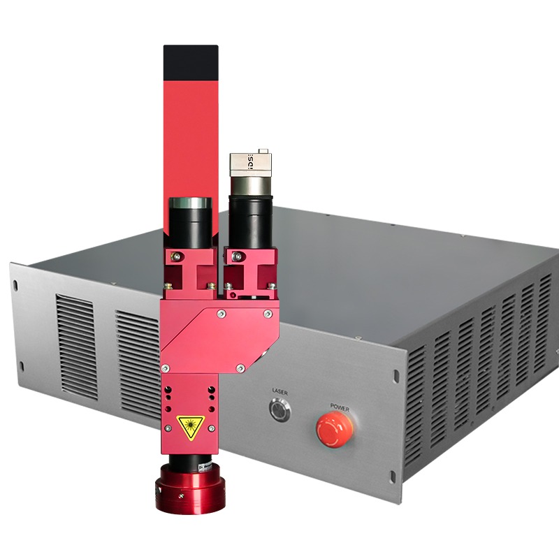
DYNALAS Laser System for Semiconductor Manufacturing Applications
Second, the three primary application scenarios of laser welding are as follows:
1. Advanced Packaging: Transitioning from 2.5D to 3D Stacking
In the manufacturing of High Bandwidth Memory (HBM), laser soldering is employed for micro-bump interconnections with silicon through-silicon vias (TSVs). Samsung’s 3D stacking technology facilitates the vertical integration of 8-layer DRAM through laser welding, achieving data transfer rates that exceed 6.4 Gbps while reducing power consumption by 30%.
2. Power Semiconductors: The Heart of Electric Vehicles
Silicon carbide (SiC) and gallium nitride (GaN) devices necessitate packages that are resistant to high temperatures and offer high reliability.
3. Optoelectronic Chips: The Key to 5G and Data Centers
Laser welding in photonic integrated circuits (PIC) is employed to achieve low-loss coupling between optical fibers and chips.
Finally, let’s discuss industry trends and challenges.
1. Breakthroughs in Ultrafast Laser Technology
Femtosecond lasers’ material melting and facilitates direct atomic-level bonding. A team of researchers at MIT has utilized this technology to integrate two-dimensional materials, such as graphene, with silicon-based chips, paving the way for advancements in quantum computing.
2. Challenges of Cost and Standardization
Despite technological advancements, the high cost of laser equipment (exceeding $500,000 per unit) continues to pose a barrier for small and medium-sized enterprises (SMEs).
Conclusion
From smartphones to autonomous vehicles, laser welding technology is transforming the future of the semiconductor industry. Despite the challenges, its advantages—precision, efficiency, and flexibility—have been validated by industry leaders such as TSMC and Intel. In the near future, it is likely that every device we use will be more powerful and reliable due to this innovative.