Flip Chip connects chips to substrates directly via bumps (Bump), replacing traditional Wire Bonding (Wire Bonding). It enables higher-density I/O (over 1,000 solder joints per square millimeter), shorter electrical signal paths (reducing inductance by 50%), and improved thermal performance.
2.Limitations of Traditional Reflow Soldering
Thermal stress issues: Bulk heating causes substrate warpage (CTE difference up to 3-5 ppm/°C);
Low process efficiency: Batch reflow requires 30-60 minutes, which cannot meet the demands of high-density packaging;
Insufficient precision: A positioning error of ±20μm limits the application of micro-bumps (μBump).
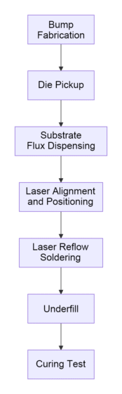
3.Advantages of Laser Reflow Soldering
Localized precise heating: The laser beam (wavelengths of 980nm/1064nm) is focused to a 50μm² area, enabling micro-area melting;
Temperature gradient control: Heating rate >100°C/s, with peak temperature 30% lower than traditional processes (220-260°C);
Contactless processing: Avoids mechanical stress damage to ultra-thin chips (<50μm).
 DYNALAS