 DYNALAS
II. LAB Technology: Redefining Optical Module Bonding Processes Through Three Key Dimensions
1. Overview of LAB Technology
Laser-Assisted Bonding (LAB) is an advanced material joining technology that utilizes lasers as a heat or energy source to achieve high-precision bonding between materials. By integrating the high energy density, localized heating, and rapid control capabilities of lasers, LAB technology exhibits broad application prospects in fields such as microelectronic packaging, semiconductor device manufacturing, and optoelectronic integration. It is particularly suitable for bonding heat-sensitive materials or those requiring high-precision positioning.
2. Key Factors for Achieving High-Quality LAB
A) Beam Spot Shaping Technology
To achieve optimal LAB results, Gaussian beam spots are typically reshaped into flat-top beam spots (see Figure 1). This effectively prevents localized overheating during bonding, which could damage the chip. Additionally, the energy distribution of the beam spot must exhibit high sharpness—meaning the edges of the beam spot need to be extremely steep—to minimize thermal impact on surrounding components or substrates (see Figure 2). Furthermore, the size and shape of the beam spot should closely match the chip dimensions to avoid unnecessary laser exposure to the chip.
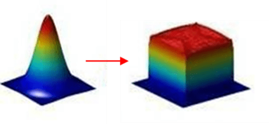
Figure 1: Gaussian Beam Spot Reshaped into a Top-Hat Beam with Uniform Energy Distribution and Steep Edges
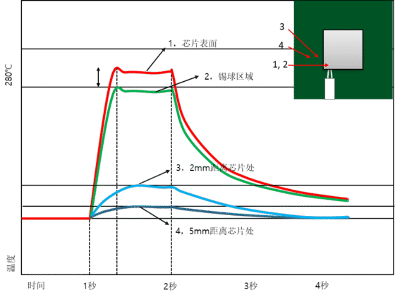
Figure 2: Test of Temperature Effects Around the Chip
B) High-Speed Closed-Loop Temperature Control
Temperature (i.e., the temperature curve) plays a critical role in bonding quality (see Figure 3). In practical applications, due to the laser’s high speed and ability to generate massive energy in short periods, temperature control systems must respond within an extremely short timeframe, with a recommended frequency of around 10 kHz. Moreover, the accuracy and repeatability of temperature control are vital. Most systems rely on infrared radiation for temperature measurement, but infrared signals are susceptible to environmental noise. Thus, the temperature measurement system must be highly reliable to process these signals effectively, ensuring accurate and consistent temperature control. Additionally, since different chips have varying emissivities, the temperature control system must adjust in real time. Finally, a coaxial laser head is recommended to precisely integrate laser, temperature control, and vision systems, achieving superior performance (see Figure 4).
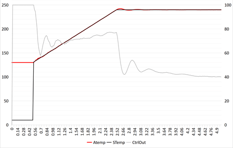
Figure 3: Real-Time Temperature Curve in High-Speed Closed-Loop Temperature Control
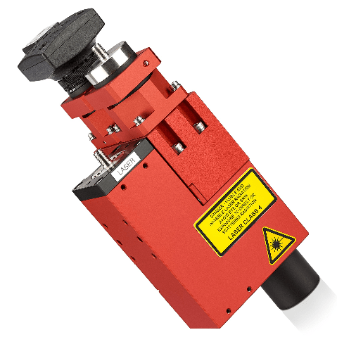
Figure 4: Coaxial Laser Head
C) Process Control
Process control is of significant importance in laser-assisted bonding. Different chips have distinct requirements for heating rates (heating curves), cooling rates (cooling/annealing curves), and bonding durations. This necessitates real-time, efficient control over the entire process. By integrating technologies such as AI, relevant process data can be analyzed and processed to further optimize parameters and enhance bonding quality.
III. Advantages of LAB Technology
Compared to traditional reflow oven processes, LAB technology can accommodate thinner, denser, and larger chips (consistent with the trend of future advanced packaging). It also delivers higher bonding quality, lower thermal stress, no impact on the surrounding environment, and greater energy efficiency, smaller footprint, and lower operational costs (see Figure 5). When compared to thermocompression bonding, laser-assisted bonding (LAB) offers advantages such as higher efficiency, lower energy consumption, and self-correction capabilities during non-contact bonding (see Figure 6). Additionally, its applications are more flexible: lasers can irradiate chips from above, below, or both simultaneously.
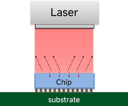
Figure 5: Schematic Diagram of Laser-Assisted Bonding
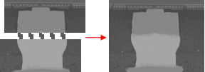
Figure 6: Self-Correction of Bonding Position
Across key performance metrics—including thermal conductivity, heat-affected zone, signal loss, processing precision, mass production yield, and process speed—LAB technology outperforms traditional processes (specific data are shown in Table 1). This indicates that LAB technology significantly enhances optical module performance and production efficiency, making it a promising candidate to become one of the mainstream processes in future optical module manufacturing.
| Parameter | Silver Epoxy Mounting | Eutectic Soldering | Thermocompression Bonding | LAB |
| Thermal Conductivity (W/(m·K)) | 20-30 | 80-100 | 100-120 | 80-150 |
| Heat-Affected Zone (HAZ) | >500μm | 300-500μm | 100-150μm | <50μm |
| Signal Loss @ 112 GHz | >3dB | 1.0-1.5dB | 0.8-1.2dB | 0.5-1.0dB |
| Processing Precision (μm) | ±50 | ±10-20 | ±10 | ±1-5 |
| Mass Production Yield (%) | 92 | 95-98 | 97 | 99 |
| Process Speed (Points/Second) | 10 | 20 | 50 | 50-200 |
Table 1: Performance Comparison Between LAB and Traditional Processes
IV. Case Studies
1.An overseas company applied LAB technology for bonding in its chip manufacturing process. After picking up the chip and placing it on a silicon wafer, the laser system heated and bonded the chip from the bottom of the wafer. This process significantly improved bonding efficiency, had no impact on surrounding components, and effectively enhanced product quality and production efficiency (see Figure 7).
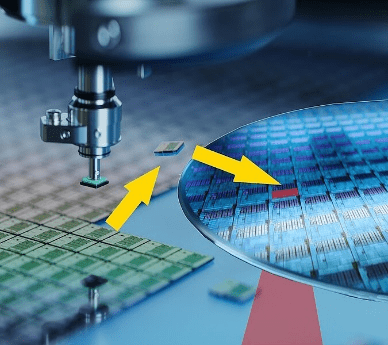
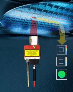
Figure 7: Bonding Using LAB Technology During Chip Manufacturing
2.A domestic company applied LAB technology when bonding flip chips to substrates in the manufacturing of high-speed optical modules (see Figure 8). Practical results show that LAB technology can drastically boost bonding efficiency and offers advantages such as high processing precision and minimal warping stress, thereby significantly improving product yield rates, reducing production costs, and enhancing the company’s market competitiveness.
Figure 8: Applying LAB Technology to Bond Flip Chips to Substrates in the Manufacturing of High-Speed Optical Modules