 DYNALAS
The Battle for Precision in Semiconductor Testing
With the rapid evolution of semiconductor devices towards processes below 5 nanometers and the development of 3D stacked packaging, probe cards—serving as the critical “bridge” for wafer testing—are encountering unprecedented challenges. These challenges include achieving micron-level solder joint precision, maintaining high-frequency signal stability, and managing thermal stress. Traditional soldering techniques are increasingly inadequate to meet these demands. In contrast, Laser-Assisted Bonding (LAB), known for its precision, efficiency, and non-contact capabilities, is emerging as the key solution to overcoming the obstacles in probe card manufacturing.
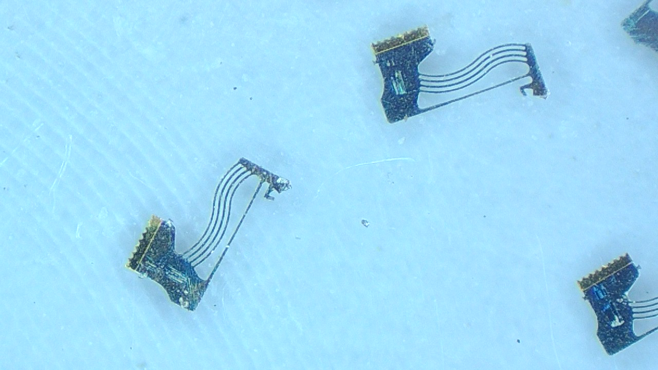
Probe card under the microscope
1. Core Advantages of Laser-Assisted Welding (LAW)
“Precision welding technology as precise as a scalpel.
- Micron-Level Precision: The laser focus diameter can be as small as 30 microns, precisely aligning with the welding requirements of ultra-fine spaced cantilever spring pins for MEMS probes. This approach mitigates the risk of displacement commonly associated with traditional welding methods.
- Localized Heating, Zero Thermal Damage: The temperature is precisely controlled in the target area (e.g., 200-300°C), enabling the safe welding of components with significant differences in thermal expansion coefficients, such as silicon-based MEMS probes.
- Non-Contact Flexible Processing: This technology can access narrow areas that traditional tools cannot reach, supporting customized linear, square, and multi-point laser beams to accommodate complex probe configurations.
2. Advantages of Laser-Assisted Welding (LAW) in MEMS Probe Card Manufacturing
LAB is a non-contact heating method designed for vertical probes or cantilever probes. Compared to traditional welding techniques, this technology offers several advantages:
- It meets the stringent precision requirements necessary for micro-welding applications, making it an ideal choice for increasingly compact packaging.
- Non-contact heating minimizes the risk of damaging delicate components.
- The shape of the laser beam can be customized (e.g., linear, square, rectangular, or dual-point), making it suitable for specific probe and test card configurations.
- Welding can be conducted in narrow or hard-to-reach areas that traditional heating tools cannot access.
Advanced laser welding technologies, including multi-point methods, can significantly reduce production time and enhance welding quality. These innovations have made laser welding increasingly popular in semiconductor and microelectronics manufacturing. The video demonstrates the actual effects of our laser system on welding probe cards.
3. Overcoming the Bottleneck Challenges in 2.5D/3D Packaging Testing
The Three Major Challenges of Advanced Packaging and LAB’s Solutions
- Fine pitch soldering: Laser technology can effectively manage pads smaller than 50 microns, thereby satisfying the dense interconnection requirements of High Bandwidth Memory (HBM).
- Thermal Management Issues: Localized heating prevents an overall increase in temperature, thereby avoiding delamination of interlayer materials caused by thermal expansion.
- High-Frequency Testing Stability: The probe impedance consistency of LAB soldering achieves ±2%, ensuring accurate testing of millimeter-wave and RF chips.
4. The Future of LAB Technology: From Cost-Cutting Solution to Industry Engine
The Multiplier Effect of Cost Reduction and Efficiency Improvement
- Cost Savings: The lifespan of LAB welding probe cards has been extended threefold, with the cleaning cycle increased from 100,000 to 300,000 uses. This enhancement has resulted in a reduction of annual maintenance costs by millions of dollars.
- Testing Revolution: Supports wafer-level system testing (WLT) and screens defective chips before packaging, reducing scrap costs by 50%.
- Technological Extension: The integration of LAB and AI visual positioning facilitates fully automated welding, with precision errors controlled within ±5 microns.
Industry Prediction: By 2028, 80% of high-end probe card manufacturing will incorporate laser-assisted welding technology.
Conclusion: Precision Drives Competitiveness—LAB Launches a New Era of Testing
In today’s world, as Moore’s Law in the semiconductor industry approaches its physical limits, the performance of probe cards plays a crucial role in determining the efficiency and cost of chip testing. Laser-Assisted Bonding (LAB), known for its micron-level precision and uncompromising reliability, is transforming the fundamental principles of semiconductor testing—from MEMS probes to 3D IC packaging, and from laboratory innovations to mass production. LAB technology serves not only as a manufacturing tool but also as the driving force propelling the industry toward greater integration and reduced testing costs.