 DYNALAS
1. Industry Pain Points and Technological Innovation
With the surge in demand for miniLED screens in fields such as consumer electronics, automotive displays, and high-end televisions, manufacturers are facing two core challenges: low mass transfer efficiency and yield loss due to insufficient bonding precision. Traditional processes rely on mechanical pick-and-place or thermal compression bonding, which can lead to issues such as chip displacement and pad damage, making it difficult to meet the manufacturing requirements for high-density, miniaturized miniLEDs.
Laser-assisted bonding technology, through non-contact processing and precise temperature control, has become the key to overcoming industry bottlenecks—this technology can control bonding precision at the micron level while achieving high-speed bonding of hundreds of chips per second.
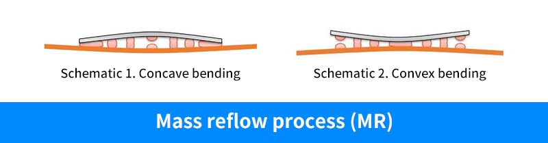
In the traditional high-volume reflow soldering process, high thermal stress can lead to warping, resulting in three types of defective solder joints:
- Non-wet solder joints – see the edge of Figure 1 and the middle of Figure 2;
- Tensile solder joints – see Figures 1 and 2;
- Bridge joints – see the middle of Figure 1 and the edge of Figure 2.

(LAB) Low thermal stress during welding and good weld joints.
2. Analysis of technical advantages
- High-precision alignment, zero-damage bonding
The laser-assisted system accurately matches the chip pads with the substrate electrodes through optical positioning and intelligent algorithms with an error of less than ±1.5 μm35. The laser energy only acts on the bonding adhesive layer, avoiding thermal stress damage to the miniLED chip and ensuring the stability of light-emitting performance. The laser energy only acts on the bonding adhesive layer, avoiding thermal stress damage to the miniLED chip and guaranteeing the stability of light-emitting performance. - High efficiency and huge amount of transfer, reduce cost and increase efficiency
The traditional process can only handle dozens of chips in a single transfer, while the laser technology can synchronize the bonding of thousands of miniLEDs, and the efficiency is increased by more than 20 times. For example, a million chips on a 6-inch wafer can be bonded with high precision within a few hours, significantly reducing unit production costs. - Closed-loop temperature control, yield rate exceeds 95%
laser system adopts closed-loop temperature control technology, real-time monitoring and adjusting the temperature of the bonding area, to ensure that the pad alloy is uniformly melted. Compared with the traditional hot pressing process, the bonding yield is increased from 80% to more than 95%, and there is no residual adhesive pollution.
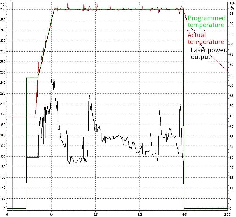
Laser welding systems with closed-loop temperature control can change the process temperature through high-speed closed-loop control of pyrometer feedback, allowing the target area to reach a predetermined temperature profile.
3.Application Scenarios and Customer Value
- Consumer Electronics: Ultra-thin miniLED backlight module
Laser bonding technology supports the processing of 0.2mm ultra-thin glass substrate, helping cell phones and tablet PCs to realize thinner and lighter display design, and at the same time, ensuring the reliable bonding of multi-million chips. - Automotive Display: High Reliability Requirements
In the vibration, temperature difference in the automotive environment, laser bonding process by strengthening the pad bonding force, so that the screen life increased by 30%, to meet the requirements of automotive-grade certification. - Wearable devices: flexible display breakthrough
Combined with flexible substrates, laser technology can complete the non-destructive bonding of curved miniLED arrays, providing high-resolution flexible screen solutions for smart watches and AR glasses.
4. Case evidence: efficiency and effectiveness of double enhancement
A head panel enterprise introduced laser-assisted bonding equipment, miniLED production line to realize:
- Capacity increase: single-day production increased from 50,000 to 120,000 pieces
- Cost reduction: bonding link energy consumption reduced by 40%, 25% reduction in material loss
- Customer Expansion: Successfully entered the Apple supply chain system after the yield rate reached the standard.
5. Future Outlook
With the continuous iteration of laser wavelength control and spot modulation technology, laser-assisted bonding will further evolve to nanometer precision and fully automated production lines. According to industry forecasts, in 2025 the global miniLED laser equipment market size will exceed 5 billion U.S. dollars, advance layout will seize the technology high point.