 DYNALAS
1. Technical Principle
Laser soldering with paste is a micro-area welding technology based on precise control of laser energy, and its core mechanisms include:
- Selective heating: Laser beams (wavelength 900-980 nm) are focused onto the solder paste area (spot size of 50-500 μm), causing the solder to melt instantaneously (138-350°C), while other areas of the substrate remain at a low temperature (<100°C);
- Metallurgical bonding: Metallurgical reactions occur between the molten solder and the pad/component pins, forming a dense alloy layer (e.g., Cu-Sn, Ni-Ag) to ensure electrical conductivity and mechanical strength;
- Dynamic protection: Purging with inert gas (nitrogen/argon) suppresses oxidation, resulting in a porosity rate of <5%.
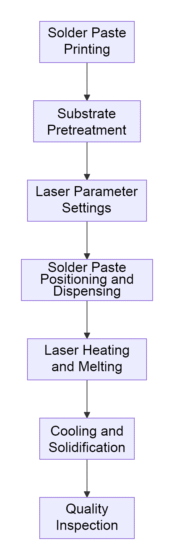
2.Process Flow
Key Step Analysis:
① Solder Paste Printing
- Using SMT stencils or micro-dispensing technology, with thickness controlled within ±2μm;
- Solder paste types: Sn42Bi58 (melting point 138°C), Sn96.5Ag3Cu0.5 (melting point 217°C).
② Laser Parameter Settings
- Energy density: 10⁵~10⁶ W/cm² (balancing melting depth and thermal damage);
- Pulse width: 0.1-10 ms (short pulses reduce thermal accumulation);
- Wavelength matching: AuSn absorption peak at near-infrared band (1064 nm).
③ Cooling Control
- Gradient cooling: 5°C/s to room temperature, suppressing residual stress;
- Nitrogen purging: Prevent oxidation and solder splashing.
3.Comparison of Technical Advantages
| Indicators | Traditional Reflow Soldering | Laser soldering with paste | Improvement Amplitude |
|---|---|---|---|
| Heat Input | >200J/mm² | <50J/mm² | Reduce by 75% |
| Heat-Affected Zone (HAZ) | >100μm | <10μm | Reduce by 90% |
| Porosity | 10-30% | <5% | Reduce by 80% |
| Minimum Weld Spot Size | 50μm | 10μm | Reduce by 80% |
| Applicable Material Combinations | Same Metal | Dissimilar Metals (e.g., Cu-Au) | Expanded Application |
4. Typical Application Scenarios
① High-Density Electronic Assembly
- Camera Module: VCM motor and lens holder welding, positioning accuracy ±0.1μm;
- FPC Connector: Laser welding of flexible board and rigid board, tensile strength >50MPa.
② Automotive Electronics
- Sensor Packaging: MEMS pressure sensor bonding with substrate, vibration resistance increased by 3 times;
- Wire Harness Welding: Welding of dissimilar materials (Cu-Al), contact resistance <0.1mΩ.
③ Optical Communication Modules
- Laser Diode Packaging: InP laser chip bonding with silicon photonic waveguide, coupling efficiency >85%;
- TO Package: Optical fiber welding with metal ferrule, hermeticity <1×10⁻⁸ atm·cc/s.